Increasing the handprint of digitalization
Chip Zero theme “Increasing the handprint of digitalization”
Interview with theme lead Safdar Muhammad

Who are you and what is your role at Applied Materials?
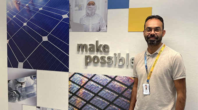
I am Muhammad Safdar, a highly accomplished chemist with a PhD in chemistry from the University of Eastern Finland. At Applied Materials in Finland, I am leading the charge in advancing Atomic Layer Deposition (ALD) technologies.
What are your particular interests in your role?
Within the realm of ALD, I am particularly interested in developing new films and ALD tools and technologies that can propel the semiconductor wafer processing industry forward.
What are the objectives of the theme you lead within the Chip Zero project?
The primary objective is to improve the efficiency of power components for electrification. We aim to achieve this by combining ALD with other technologies and studying the performance improvements at both the component and system levels.
What are the key research questions and challenges in the roadmap related to this theme?
The roadmap presents several key research questions and challenges. We aim to explore how ALD and related technologies can enhance the properties of films at the nano level, particularly at the surface or interface level. Additionally, we aim to integrate these chips into larger systems, such as power grids and EV charging stations, to improve overall power efficiency and device lifetime.
How does your theme support the program's major goals?
While other themes focus on improving ALD equipment manufacturing efficiency and boosting circularity, my theme focuses on the devices made using ALD. By enhancing the efficiency of power components through ALD, we contribute to the overall goal of achieving a more sustainable semiconductor industry.
What is Applied Materials planning to do in relation to the Chip Zero project?
Applied Materials aims to build an ecosystem through various conversion projects within the context of the Chip Zero program. These projects will study the interfacial properties of ALD-deposited films to improve power component efficiency. Additionally, we are working on a co-innovation project and collaborating with ecosystem partners to enable neuromorphic computing applications that consume less power. We are also collaborating with universities and power component suppliers in Finland to develop a system that can efficiently manage power demand fluctuations.
Where specifically is the contribution of partners needed in the ecosystem?
To achieve our goals, we recognize the importance of collaboration with partners. We require the expertise of academia involved in power management systems development. Collaboration with power component chip manufacturers and industry players involved in EV applications, such as charging units and power storage systems, is also crucial. By building an ecosystem that fosters collaboration, we can test and refine the technologies we develop, ultimately benefiting consumers at the application level.
Do you already have potential partners in mind for collaboration/project concepts?
Yes, Applied Materials has already identified potential partners for collaboration and is actively building the ecosystem around this theme. We are in the early stages of developing a project with the University of Tampere and power partner Danfoss, showcasing the strong interest and support from these partners.
How is Applied Materials revolutionizing the semiconductor industry through ALD?
Applied Materials is revolutionizing the semiconductor industry by pushing the boundaries of what is possible with ALD. Through our commitment to innovation and the development of new films, ALD tools, and technologies, we are driving advancements in conductor wafer processing. By enhancing the efficiency and sustainability of power components, we are contributing to a more efficient and sustainable future for the semiconductor industry.
